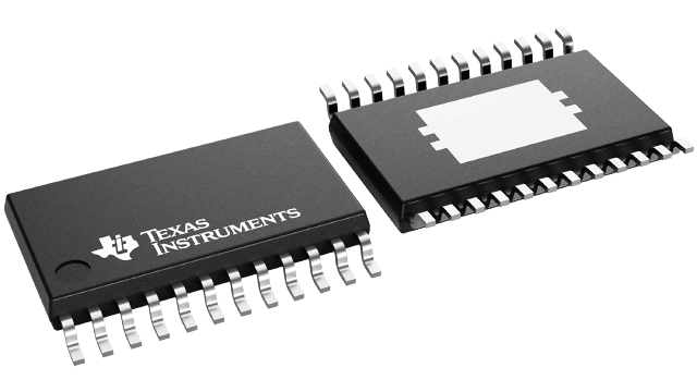
Información de empaque
| Encapsulado | Pines HTSSOP (PWP) | 24 |
| Rango de temperatura de funcionamiento (℃) -40 to 125 |
| Cant. de paquetes | Empresa de transporte 2,000 | LARGE T&R |
Características para TPS92663A-Q1
- AEC-Q100 qualified for automotive applications
- Device temperature grade 1: –40°C to 125°C TA
- Device HBM classification level: H1C
- Device CDM classification level: C5
- Input voltage range: 4.5 V to 60 V
- Six integrated bypass switches
- Two sub-strings of three series switches
- 20-V (maximum) across switch
- 62-V (maximum) switch to GND
- Multi-drop UART communication interface
- Up to 16 addressable devices
- Integrates on same bus with TPS92662A-Q1
- Compatible with CAN physical layer
- Minimum number of wires in cable harness
- 8-bit ADC with two MUX inputs
- Crystal oscillator driver
- Programmable 10-bit PWM dimming
- Individual phase shift and pulse width
- Device-to-device synchronization
- LED open and short detection and protection
Descripción de TPS92663A-Q1
The TPS92663A-Q1 LED matrix manager device enables fully dynamic adaptive lighting solutions by providing individual pixel-level LED control.
The device includes two sub-strings of three series-connected integrated switches for bypassing individual LEDs. The individual sub-strings allow the device to accept either single or multiple current sources. It also allows a parallel connection of two switches to bypass high-current LEDs.
A primary microcontroller controls and manages the TPS92663A-Q1 devices via a multi-drop universal asynchronous receiver transmitter (UART) serial interface. The serial interface supports the use of CAN transceivers for a more robust physical layer. An application may use the TPS92663A-Q1 device and the TPS92662A-Q1 device on the same bus.
An on-device, 8-bit ADC with two multiplexed inputs can be used for system temperature compensation and used to measure a binning value which allows for LED binning and coding.
The internal charge pump rail supplies the gate drive voltage for the LED bypass switches. The low on-resistance (RDS(on)) of the bypass switch minimizes conduction loss and power dissipation.
The phase shift and pulse width for each individual LED in the string are programmable. The device uses an internal register to adjust the PWM frequency. Multiple devices can be synchronized. The switch transitions during PWM dimming operation have a programmable slew rate to mitigate EMI concerns. The device features open LED protection with programmable threshold. The serial interface reports open LED or short LED faults.
