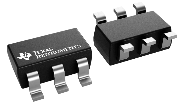
封裝資訊
| 封裝 | 引腳 SOT-23 (DBV) | 6 |
| 作業溫度範圍 (°C) -40 to 125 |
| 包裝數量 | 運送包裝 3,000 | LARGE T&R |
TPS22917 的特色
- Input operating voltage range (VIN): 1 V to 5.5 V
- Maximum continuous current (IMAX): 2 A
- On-resistance (RON):
- 5 VIN = 80 mΩ (typical)
- 1.8 VIN = 120 mΩ (typical)
- 1 VIN = 220 mΩ (typical)
- Ultra-low power consumption:
- ON state (IQ): 0.5 µA (typical)
- OFF state (ISD): 10 nA (typical)
- Smart ON pin pulldown (RPD):
- ON ≥ VIH (ION): 10 nA (maximum)
- ON ≤ VIL (RPD): 750 kΩ (typical)
- Adjustable turn ON limits inrush current
(tON):
- 5-V tON = 100 µs at 72 mV/µs (CT = open)
- 5-V tON = 4000 µs at 2.3 mV/µs (CT = 1000 pF)
- Adjustable output discharge and fall time:
- Optional QOD resistance ≥ 150 Ω (internal)
- Always-ON true Reverse Current Blocking (RCB):
- Activation current (IRCB): –500 mA (typical)
- Reverse leakage (IIN,RCB): –1 µA (maximum)
TPS22917 的說明
The TPS22917x device is a small, single channel load switch using a low leakage P-Channel MOSFET for minimum power loss. Advanced gate control design supports operating voltages as low as 1 V with minimal increase in ON-Resistance and power loss.
The Rise and Fall times can be independently adjusted with external components for system level optimizations. The timing capacitor (CT) and turn on time can be adjusted to manage inrush current without adding unnecessary system delays. The output discharge resistance (QOD) can be used to adjust the output fall time. Connect the QOD pin directly to the output for a fastest fall time or leave it open for the slowest fall time.
The switch ON state is controlled by a digital input that can interface directly with low-voltage control signals. The TPS22917 uses active high enable logic, while the TPS22917L uses active low. When power is first applied, a Smart Pulldown is used to keep the ON pin from floating until system sequencing is complete. After the ON pin is deliberately driven high (≥VIH), the Smart Pulldown (RPD) is disconnected to prevent unnecessary power loss.
The TPS22917x device is available in a leaded SOT-23 package (DBV) which allows visual inspection of solder joints. The device is characterized for operation over a temperature range of –40°C to 125°C.
