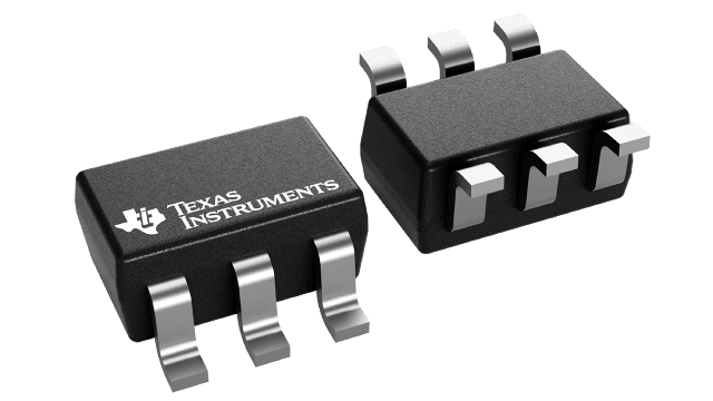
Gehäuseinformationen
| Gehäuse | Pins SOT-SC70 (DCK) | 6 |
| Betriebstemperaturbereich (°C) -40 to 125 |
| Gehäusemenge | Träger 3.000 | LARGE T&R |
Merkmale von LM66100
- Wide operating voltage range: 1.5 V – 5.5 V
- Reverse voltage standoff on VIN:
–6-V absolute maximum - Maximum continuous current (IMAX): 1.5 A
- On-Resistance (RON):
- 5-V VIN = 79-mΩ (typical)
- 3.6-V VIN = 91-mΩ (typical)
- 1.8-V VIN = 141-mΩ (typical)
- Comparator chip enable (CE)
- Channel status indication (ST)
- Low current consumption:
- 3.6-V VIN Shutdown current (ISD,VIN): 120-nA (typical)
- 3.6-V VIN Quiescent current (IQ, VIN): 150-nA (typical)
Beschreibung von LM66100
The LM66100 is a Single-Input, Single-Output (SISO) integrated ideal diode that is well suited for a variety of applications. The device contains a P-channel MOSFET that can operate over an input voltage range of 1.5 V to 5.5 V and can support a maximum continuous current of 1.5 A.
The chip enable works by comparing the CE pin voltage to the input voltage. When the CE pin voltage is higher than VIN, the device is disabled and the MOSFET is off. When the CE pin voltage is lower, the MOSFET is on. The LM66100 also comes with reverse polarity protection (RPP) that can protect the device from a miswired input, such as a reversed battery.
Two LM66100 devices can be used in an ORing configuration similar to a dual diode ORing implementation. In this configuration, the devices pass the highest input voltage to the output while blocking reverse current flow into the input supplies. These devices can compare input and output voltages to make sure that reverse current is blocked through an internal voltage comparator.
The LM66100 is available in a standard SC-70 package characterized for operation over a junction temperature range of –40°C to 125°C.
